Intel’s plans to regain process leadership got a shot in the arm when their new CEO, Pat Gelsinger stepped in and laid down several measures to be implemented. A good chunk of these was unveiled at the Intel Accelerated Event held in July this year. We got to see the roadmap that Intel has laid down for itself to achieve the smallest process node in 2025. The roadmap outlines a very aggressive strategy with rapid jumps from one node to the next one while leveraging some of their existing technologies while also incorporating newer ones. And not only will Intel reap the benefits of the improvements to their process technologies but under their IDM 2.0 strategy, external customers will also get to build their silicon at Intel’s foundries. Let’s take a closer look at Intel’s plans.
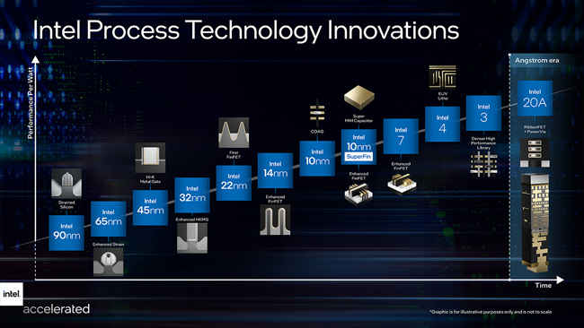
Intel Roadmap - Five process nodes in four yearsIntel like most of the other silicon manufacturers, such as TSMC and Samsung, has its own naming system. Transistors nodes were named as per the length of the transistor gates in the past but since the transistors have grown smaller, each manufacturer went ahead with their own naming systems. And since there is no industry standard as such, we’re left to simply draw parallels between the process nodes of one manufacturer with that of the other. Intel’s 14nm process was more in line with Samsung and TSMC’s 10nm processes and their newer 10nm Super Fin is close to Samsung and TSMC’s 7nm. At the Intel Accelerated event, Intel went ahead and renamed its existing and upcoming nodes. This includes naming their future nodes using Angstroms instead of Nanometers.

The current node, i.e. 10nm Super Fin (previously considered 10+) will remain as is. However, its successor, the 10nm Enhanced Super Fin (10ESF) will now be referred to as Intel 7. And its 7nm node will be called Intel 4. Similarly, 7+ becomes Intel 3, 5 becomes Intel 20A (A stands for Angstrom). And after 20A comes 18A which is still under development.
From a marketing perspective, this renaming is a huge bonus. Intel’s nodes previously seemed to be catching up even when they had process superiority back in the era of the 22nm and 14nm. This was because the competition process nodes had smaller numbers despite have similar transistor densities. With this new renaming, Intel flips that around and makes it seem like they have process superiority even if the transistor densities would be similar. Here’s a little table to summarise the naming scheme changes.
Old Node Name
New Node Name
Year
Type
10
10
2019
FinFET
10+
10 Super Fin
2020
FinFET
10 Enhanced Super Fin
7
2021
FinFET
7
4
2022
FinFET
7+
3
2023
FinFET
5
20A
2024
Horizontal Nanosheets
5+
18A
2025
Horizontal Nanosheets
We can see that there is a new process node being put into production. Some of the products are already known to us. Alder Lake i.e. Intel 12th Gen Core processors will be the first to be built on the new ‘Intel 7’ node and the same will be used in the Sapphire Rapids products coming to the data centre in 2022. ‘Intel 4’ will be used in Meteor Lake and Granite Rapids, and so on. Each new node will bring with it a lot of improvements and it’s easier to summarise them in a point-wise fashion.
Intel 10 SuperFin (10SF)
Currently used for Tiger Lake, Xe-LP (SG1, DG1), Xe-HPC Ponte Vecchio
Intel 7 (Previously 10 Enhanced SuperFin)
10-15% more performance-per-watt over 10SF
Will be seen in 12th Gen Core Alder Lake (2021) and Sapphire Rapids (2022)
Intel 4
20% more performance-per-watt over ‘Intel 7’
Will see EUV lithography being used
WIll be seen in 13th Gen Core Meteor Lake (2023) and Granite Rapids (2023)
Intel 3
18% more performance-per-watt over ‘Intel 4’
Denser higher-performance library over ‘Intel 4’
Increased use of EUV lithography
Increased intrinsic driver current
Optimised interconnect metal stack
Ready in the latter half of 2023 and used in products in 2024
Intel 20A
Will switch from FinFET to Horizontally Stacked Gate-All-Around Nanosheets (Intel calls these RibbotFETs)
Will introduce a Backside Power Delivery mechanism called PowerVia
Ready in the first half of 2024
Intel 18A
Ready in the first half of 2025
Up until 20A, everything is progressing normally with improvements being made to the way FinFETs are being used in building smaller and denser process nodes. FinFET’s limitations will be realised at that point and the industry as a whole will move towards using Horizontally Stacked Gate-All-Around Nanosheets.
Intel RibbonFETEvery manufacturer likes to call Horizontally Stacked Gate-All-Around Nanosheets using a different term. The industry knows them as GAAFET or Gate-All-Around-FET but Samsung uses the term Multi-Bridge Channel FET or MBCFET whereas TSMC will continue to stick to FinFETs well into their 3nm process so they haven’t revealed what they would be calling it. Intel will use the term RibbonFET. The technology isn’t new. In fact, the first-ever GAA-FET was demonstrated back in 1986. But making GAA-FET small enough and packing them in a dense structure took more than three decades.
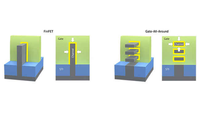
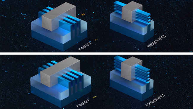
RibbonFET uses Ribbon-shaped channels which are surrounded by the gate on all sides, hence, gate-all-around. This enables much better control and helps archive a higher drive current at all voltages. So transistors can switch faster and that inevitably means that performance gets a bump. The following images might help you better understand where the benefits lie.

On the left, we have a typical FinFET design and on the right, you’ve got GAA-FET. In FinFET, you’ve got the gate interfacing with the channels on three sides whereas, with GAA-FET, even the fourth side makes contact with the gate. This results in the higher level of control that we previously mentioned.
The benefits of RibbonFET become more apparent as you scale the designs. With FinFETs, you can scale by increasing the number of fins which inadvertently increases the area used by the transistor. Whereas with RibbonFET, you can add stack another ribbon in the same space and get a higher drive current. Essentially, you can get more done in the same space.

So if processors need to grow smaller and silicon manufacturer’s need to keep Moore’s Law alive, then GAA-FET is the way to go.
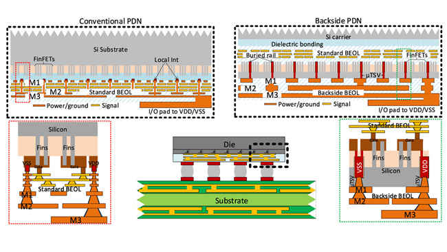
Intel PowerViaAnother interesting technology being introduced in the Intel 20A process is Intel PowerVia or what the industry calls Backside Power Delivery. Traditional silicon chip manufacturing consists of layers upon layers of metal and other substances. The communication interface and power supply for these chips are given from the same surface. We’ve seen how a delidded processor looks like, it’s just a package slapped onto a substrate. On the inside of these chips, you’ve got all the different layers. When the power supply comes in from the topmost layer, then by the time it reaches some of the lower layers, it loses out a lot of power because of wire resistances and other parasitic capacitances. The power delivery network has to content for space alongside the signal wires.
This problem is solved by supplying power from the bottom layer and then channelling power to the higher layers using thicker wires or (Through Silicon Via) TSVs. Now chips will have wiring on both sides with signal wires on one end and power wires on the other. The transistors will get sandwiched between these two layers.

With PowerVia, you no longer have the Power Delivery Network (PDN) contending with the signal wires for space. Nor is it that big a source for interference anymore. This leaves room for the signal wires to be better optimised.
To get more information on RibbonFET, PowerVIA and Intel’s aggressive growth plans, we reached out to Intel with a few queries. Deemanth Nagaraj, Intel Fellow was more than accommodating while answering our queries. Here’s what Intel had to say.

Digit - What are the challenges that PowerVia is meant to resolve? Is it explicitly linked to RibbonFET or are the two independent of each other?
Intel - PowerVia will be an industry-first deployment of a backside power delivery network technology when it is introduced with Intel20A. It significantly reduces the need for power routing on the front side of the wafer by bringing power in from the backside, making more resources available for optimizing signal routing and as a result, reducing signal delays. The overall result is a performance boost at the IP block level and a reduction in power leakage.
PowerVia is independent of RibbonFET, which is Intel’s implementation of the Gate All Around transistor. We expect to test PowerVia on earlier nodes to ensure this groundbreaking technology is fully ready before it ramps in volume with Intel 20A in 2024. We also expect first product for PowerVia to be a leadership client solution.
Digit - ASML announced a delay of 3 years (https://ift.tt/3ijkZ0o) for their High-NA machines to hit production. Will that affect Intel's 20A or 18A plans?
Intel - We can’t comment on speculative reports. We can say that Intel is positioned to receive the first High NA EUV tool in the industry, and we are driving to enable its introduction in 2025. We have a very strong partnership with EUV equipment leader ASML, and our plans to stay on the leading edge of EUV usage are well underway.
Digit - The plans to return to process leadership seems to be quite aggressive. On top of that, you're also reducing the cadence cycle and going back to tick-tock. Isn't it an extremely risky move if you wish to release client products on newer nodes every year? Or would we see fewer client launches to allow for more time to iron out each node?
Intel - Intel continues to compete and win in our core PC market with a steady drumbeat of highly competitive CPU and platform innovation. We are laser focused on delivering a predictable yearly cadence of innovation and are well on the path to get back to our “tick tock” momentum.
The roadmap we’ve shown at Intel Accelerated is one of the most detailed roadmaps we’ve ever provided for process and packaging technologies and it shows a better than yearly cadence: 5 process nodes in 4 years! We have funded the R&D and capital for the teams and are taking all the right steps to ensure we execute at this incredible pace.
Digit - Continuing with the previous question, what kind of risk mitigation strategies (backporting?) are you implementing to ensure that your launch cycles are on schedule?
Intel - We are embracing the industry as never before in areas like equipment, EDA and research:
• We’re collaborating across our equipment suppliers to make sure we are leveraging the best from the industry. This includes a deep partnership with ASML on EUV, both in fully embracing EUV for Intel 4 and staying on the leading edge of EUV with our swift adoption of High-NA, the next major technology change on the EUV roadmap.
• We’re adopting industry-standard approaches where it makes sense, like industry-standard EDA tools and models.
• We’re building on our partnerships with leading research organizations, such as IBM, IMEC and Leti. This combined with our own components research gives us confidence that we are on very solid footing.
The ecosystem support we’ve demonstrated shows the confidence our customers and partners have on the predictable cadence that Intel is now on – including deep technical validation from customers, like the announcement with Qualcomm.
Digit - How are thermals being managed on chips using Backside Power Delivery? Is it more of an offset because the node becomes more efficient, or do you have to make changes with the way you package the chip for production?
Intel - Thermal management is a key element in all packaging configurations and is determined based on a number of inputs – die floorplan, interconnect architecture, die thickness, package configuration, to name a few – and PowerVia power delivery is one of those elements that is input into the thermal design point (TDP) calculation. Thermal solutions are ultimately determined by the best combination of thermal interface materials and system cooling solutions that meet the customer’s need. Our assembly technology is designed to be flexible so that our customers can optimize their products to manage TDP, footprint and cost. This is a key element of our IDM 2.0 strategy and one reason why we believe we have an advantage over the competition in packaging.
from PC Components News https://ift.tt/3CQLJwk


No comments:
Post a Comment